
You are using an out of date browser. It may not display this or other websites correctly.
You should upgrade or use an alternative browser.
You should upgrade or use an alternative browser.

That might be tough, What device is it in, Would need to see picture of the area round the chip and would need to see the other side of the board as well to seeing that chip has traces that go into vias.. However that might be problematic as well. Seeing I have worked on some very complex multil layer boards where the device is at top left of PCB and there is nothing on the other side just the connected hole because the trace it is going into on another layer of the PCB and ends up at the bottom center on the same side as the chip. Even some same concept with connection points to multi areas on both sides..
Sometimes without the right tools, or Schematic for working out what is what it comes down to using another of same type for probing and knowing what the chip does, VCC, VDD, PG, GND, CTL and things like that. Having a good working device can help understand what the chip is to find a replacement that don't just have some scribed in with no logo letters and numbers..
Clear High res picture with little or no reflections of both sides of board with some cross reference to know the correct position of the chip on the other side.. For me, I would take picture, Flip right to left not bottom to top but from right to left.. This keeps the pins at the bottom still at the bottom. If you were to flip bottom to top or top to bottom it will change the position of the pins.. Pain for trying to trace.. Also if you happen to have a high power light that you could run under the chip to try and help see if there is hidden in layer would help as well..

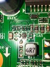
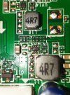
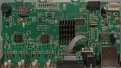
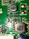
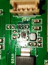
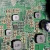
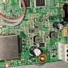
This is hikvision 8 port DVR the user connected the power positive in place of negative and 3 IC show damage with no sign of life on the device
Attachments
-
 IMG_20250302_173541.jpg758.4 KB · Views: 0
 -
 IMG_20250302_173512.jpg758.7 KB · Views: 0
 -
 IMG_20250302_173451.jpg583.5 KB · Views: 0
 -
 IMG_20250302_190210.jpg485.1 KB · Views: 0
 -
 IMG_20250302_173541.jpg758.4 KB · Views: 0
 -
 IMG_20250302_173511.jpg721.3 KB · Views: 0
 -
 IMG_20250302_173451.jpg583.5 KB · Views: 0
I've attached themThat might be tough, What device is it in, Would need to see picture of the area round the chip and would need to see the other side of the board as well to seeing that chip has traces that go into vias.. However that might be problematic as well. Seeing I have worked on some very complex multil layer boards where the device is at top left of PCB and there is nothing on the other side just the connected hole because the trace it is going into on another layer of the PCB and ends up at the bottom center on the same side as the chip. Even some same concept with connection points to multi areas on both sides..
Sometimes without the right tools, or Schematic for working out what is what it comes down to using another of same type for probing and knowing what the chip does, VCC, VDD, PG, GND, CTL and things like that. Having a good working device can help understand what the chip is to find a replacement that don't just have some scribed in with no logo letters and numbers..
Clear High res picture with little or no reflections of both sides of board with some cross reference to know the correct position of the chip on the other side.. For me, I would take picture, Flip right to left not bottom to top but from right to left.. This keeps the pins at the bottom still at the bottom. If you were to flip bottom to top or top to bottom it will change the position of the pins.. Pain for trying to trace.. Also if you happen to have a high power light that you could run under the chip to try and help see if there is hidden in layer would help as well.
Thanks will look over it maybe look into a place called All About Circuits as there maybe someone there that has dealt with such part. Why do you think the part is bad?
Thanks revo i had found one of the broken and the other show damageThanks will look over it maybe look into a place called All About Circuits as there maybe someone there that has dealt with such part. Why do you think the part is bad?
Yeah I see now in the last picture 78 spot blown out, these things are so small, looking at one of my DVR while have kind of same layout, mine has more inductors and are marked AUCK and ATUK. The one handy is 2-3 years older then yours. I do have one that is year older might be year newer, been awhile since I had it open so not sure board date think it's 2020.. Wonder what killed it
Some how the user tried to connect the device for 12v power supply instead of device adapter and reversed + - so this IC's get roasted :/Yeah I see now in the last picture 78 spot blown out, these things are so small, looking at one of my DVR while have kind of same layout, mine has more inductors and are marked AUCK and ATUK. The one handy is 2-3 years older then yours. I do have one that is year older might be year newer, been awhile since I had it open so not sure board date think it's 2020.. Wonder what killed it
Yeah kind of crazy that even mine done have a couple pennies protection diode for reverse protection. So I know it won't help much but will put in some area of what your looking for. Testing incoming voltage was 12v then there was 5v output with a 1.5v reference, so pin1 was 12v pin3 was 1.5v and pin6 was 5v. So it seems to be a dc-dc buck converter. So to get you in ballpark you would want to measure the package size, using a quality micrometer, not sure one from Harbor Freight would offer good enough values but might work. Then taking the size in mm with in being pin 1 a power good or reference voltage on 3 and output on 6 can get you to a chip that offers same type values and might need to measure the resistance of resistors next to it to help aid in what is offered. Plus looking at datasheets you can find what other pins will be used for.
Attachments
Thanks revo for your supportYeah kind of crazy that even mine done have a couple pennies protection diode for reverse protection. So I know it won't help much but will put in some area of what your looking for. Testing incoming voltage was 12v then there was 5v output with a 1.5v reference, so pin1 was 12v pin3 was 1.5v and pin6 was 5v. So it seems to be a dc-dc buck converter. So to get you in ballpark you would want to measure the package size, using a quality micrometer, not sure one from Harbor Freight would offer good enough values but might work. Then taking the size in mm with in being pin 1 a power good or reference voltage on 3 and output on 6 can get you to a chip that offers same type values and might need to measure the resistance of resistors next to it to help aid in what is offered. Plus looking at datasheets you can find what other pins will be used for.

Here is datasheet also match yours
Thank you for the Datasheet, however that wouldn't match my chip so that was why i was saying will have to check the datasheet to confirm if it is correct. If you look at that one you posted on page 13 it is showing Pin 5 being the input and pin 1 is a bootstrap my guess that chip wouldn't work in my device as it is working right now..
You are right this IC have different input/output also it depend on the resistance around it to set the needed volt maybe you can indicate the output that send to the coil 4R7Thank you for the Datasheet, however that wouldn't match my chip so that was why i was saying will have to check the datasheet to confirm if it is correct. If you look at that one you posted on page 13 it is showing Pin 5 being the input and pin 1 is a bootstrap my guess that chip wouldn't work in my device as it is working right now..
I had found an Arabic with en translation video show more information about it